We continue with our PCB design course by looking at some notions of how a PCB is manufactured. Although it is not really necessary for designing PCBs, it is indeed convenient to know, even slightly, about the PCB manufacturing process.
We say slightly, because we are only going to see a general and summarized idea of the manufacturing process. The complete process is a complex industrial process with multiple stages and baths, which can also have variations.
However, and within our intention to demystify and “lose the fear” of PCBs, we cannot fail to see the manufacturing process. The goal is to have some knowledge, so that PCBs are not “that magical thing that is manufactured ‘who knows how’.”
We will focus solely on the process for 2-layer PCBs, which as we know are very common and the ones we will use most frequently at a domestic level. However, the process for PCBs with more layers would be similar, but incorporating a greater number of stages for the intermediate layers.
So let’s look at this great and conceptually simple manufacturing process (of course, quite complex in practice) and which requires multiple stages perfectly orchestrated to achieve a quality product.
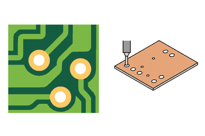
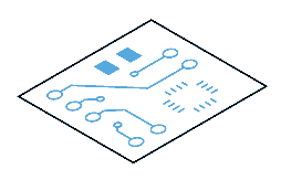
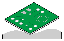
Manufacturing a 2-layer PCB
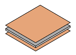
We begin this review of the manufacturing process with material lamination, which consists of adhering the upper and lower copper layers by applying temperature and pressure (on the order of 200º and 25 atmospheres).
Next, the holes are made (both for holes, vias, pads for PTH components) in the board. These holes can be made either with a CNC milling machine or by laser cutting.
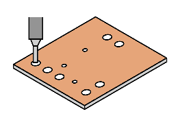
Once the board is drilled, an electroless deposition process is carried out. This coats the walls of the hole with a thin layer of copper, on the order of microns, which connects the top layer with the bottom one.
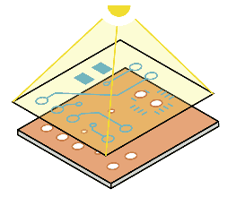
On the other hand, using high-precision printers, transparent sheets, or films, are generated that contain the design of the circuit we want to manufacture.
It is worth noting that the manufacturing process for the inner and outer layers is slightly different. Specifically, the printed films are transparent in the areas we want to remove on the inner layers, and the opposite for the outer layers.
Returning to our board, a photosensitive layer is applied to it. On top of this, the previous transparent film, which contains the circuit design, is placed, ensuring that all layers are perfectly aligned.
Next, the design is transferred to the board by isolation. For this, it is exposed to powerful ultraviolet light, which hardens the photosensitive layer only in the areas where the film is transparent.
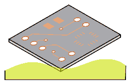
Subsequently, the board is immersed in a series of chemical baths that remove the remains of the photosensitive layer and the copper from the areas we want to remove, leaving only the corresponding areas with the circuits.
Next, the protective lacquer or Soldermask is applied. Typically, ultraviolet light is also used to prevent certain parts (the ones that will remain as solderable) from being covered by the Soldermask.
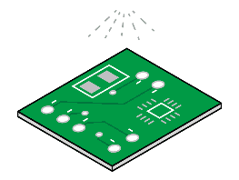
Subsequently, the board goes through a new series of baths, after which the exposed copper parts end up covered by a thin layer of tin that will facilitate the later soldering of components and, in addition, protects the copper.
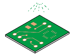
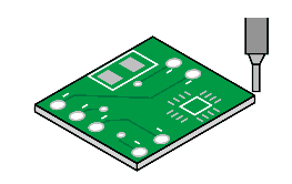
The board then goes to an ink printer, where the silkscreen with the texts and annotations is printed.
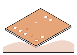
Finally, the boards are cut to their definitive shape on a CNC machine. Normally, PCBs are manufactured on larger boards, which contain several designs. This process also divides the global board into the different individual PCBs.
In summary
So, in summary, this is the basic process of building a PCB. As we can see, it is a process with multiple stages, but it is enough for us to keep the most relevant points.
- The model transfer is done by photo transfer using two sheets, one photosensitive applied to the board and another transparent one that contains the circuit design.
- Numerous baths in different chemical substances are applied, which deposit or remove the conductive materials from the areas we desire.
- There are other mechanical processes such as hole drilling, silkscreen printing, and contour machining.
All these stages, correctly combined, result in us having our little PCB in our hand. Pretty impressive, right?
And now that we have seen the basics and the manufacturing of a PCB, it’s time to start talking about the components we will mount on it, to configure our electronic circuits.
This is precisely what we will dedicate the next entry in the section to, where we will see SMD vs. PTH components, and the advantages and disadvantages of each.
