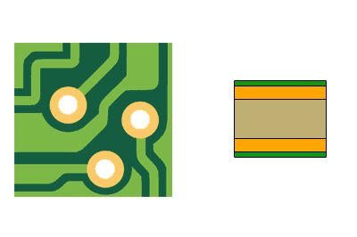
We have already mentioned that the “trick” of a PCB is that it has conductor tracks that “act as wires” to connect components, and together they make an electronic circuit.
We have also mentioned that these tracks are made using one or more layers of conductive material, usually by removing parts of a continuous layer.
Now it’s time to look in more depth at all this about conductor layers. It may seem like a headache, but we’ll tell you in advance, it’s much easier than it seems.
The layers constitute the internal (and external) structure of the PCB. And this can be very simple or become really complex. But let’s go from less to more, starting with the simplest case, which is a single conductor layer.
Single-Layer PCB
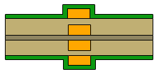
We start with the structure of a single-layer PCB, so called because it has a single outer layer of copper. If we ignore the surface paint layer (silkscreen), the internal structure of a single-layer PCB could be as follows.
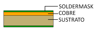
Where the substrate, the copper layer, and the solder mask layer are represented. You will find similar representations in PCB design software and on manufacturer pages to represent the internal structure of the PCB we are going to design or purchase.
However, in the PCB manufacturing process, part of the copper layer is removed to configure the circuit tracks, and subsequently, the solder mask would be applied. So, a more accurate representation of the final PCB would be something like this.
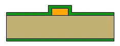
Where part of the solder mask is applied over the copper and part directly onto the substrate. That’s why you will see two shades of green (or whatever color) on the boards, with the lighter shade being where there is copper underneath.
The substrate thickness is usually between 0.8 and 1.6mm. There are several possible materials, with fiberglass with an epoxy resin being common.
You will frequently see the designation FR4 to refer to the substrate. This does not name the material itself, but rather it complies with a NEMA standard and indicates that it is flame retardant.
Regarding the copper layer, thicknesses are measured in Oz/ft^2, with 1 Oz/ft^2 and 2 Oz/ft^2 being common. To give you an idea of how thin it is, 1 Oz/ft^2 translates to a thickness of 1.37 mils (thousandths of an inch) or 0.0347 mm.
Regarding the solder mask or lacquer layer, there are also several processes. So we have HASL (Hot Air Solder Leveling), which is the one we will use most frequently because it is very cheap. Other types of solder mask, more expensive, are lead-free HASL and ENIG (Electroless Nickel)
Two-Layer PCB
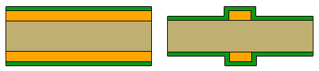
If instead of having copper on one side of the substrate, we have copper layers on both sides of the substrate, we get a two-layer PCB. In this case, our ‘standard’ representation of the PCB’s internal structure would be as follows.
Having two layers has the obvious advantage of having double the surface area, because we have two sides to make circuits. This translates into a smaller PCB for the same electrical circuit.
But the biggest advantage is that with two layers we can avoid crossovers. Imagine the following example, where four points have to be connected to another four, but the two in the middle are “crossed”.
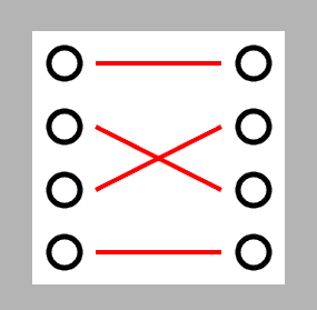
If we cannot go outside the gray area (because it is full of other components), we cannot make the circuit because two tracks cross. But if we have two layers, we can pass one of the tracks underneath (blue) and avoid the crossover.

It can be demonstrated that with two layers we can realize any circuit topology, as long as we have enough surface area. Something that, with one layer, is not possible, so they are very limited.
In general, two-layer PCBs are the most common type of board. Online services charge the same for a one-layer as for a two-layer, so we will always choose the two-layer one.
PCB with More Than Two Layers
Finally, and to conclude, there are PCBs with many more layers. There are PCB formats with 4, 8, 16, up to 64 layers. For this, the additional layers are internal layers, within intermediate substrate layers.
The intermediate layers usually have less thickness than the exterior ones. Furthermore, they can support less current because they dissipate heat worse.
Having more layers allows for very complex circuits in a much smaller space. However, their design and manufacture are also considerably more complex.
However, for now, PCBs with more than two layers are substantially more expensive than two-layer ones. Therefore, we will focus on two-layer ones and leave those with more layers for the industry (or wait a few years to see if they become cheaper someday).
Conclusion
That’s all for this entry about layers and the internal constitution of the PCB. Wasn’t it that difficult?
Now the question arises: How do we connect one conductor layer to another? That’s what we will see in the next entry where we will look at vias, an essential element in almost any PCB.
