In this post, we are going to see the parts that make up a PCB and their functionality, and we will introduce some vocabulary that we will frequently encounter when diving into this great “world” of PCBs.
So let’s start with the substrate, the most visible part of a PCB. The substrate is the body of the PCB, it is “what we touch”. The thickness is usually between 0.8 to 1.6mm. This insulating substrate base serves to support the components and conductive circuits, and to insulate them from each other.
On the substrate, there are one or more very, very, very thin layers of conductive material (on the order of hundredths of a mm), usually copper. These layers are configured into traces that make up the circuits, typically by removing certain parts from a continuous copper layer.
The traces are “little paths” of conductive material that connect the electronic components we mount on the PCB and “act as wires”. Together, PCB and components, form the electronic circuit.
As we mentioned, it is possible to have more than one copper layer. In fact, we usually have two layers, one on each side of the PCB. But it is possible to have more layers, inside the PCB itself. We will see all this in more detail in the next post, about PCB layers.
The copper layers are insulated and protected with a solder mask layer. This lacquer gives the board its characteristic color, with green, white, red, black, and blue being common colors.
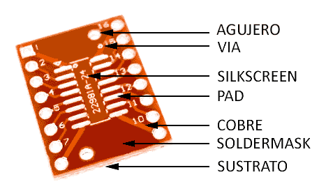
For example, in the image above we have two shades of red. The light parts are where there is copper underneath, while the dark parts are not, and the solder mask is applied directly onto the substrate.
On the other hand, we have the Pads, which are areas where we are going to mount components. The solder mask is not applied in these areas, so the copper is “exposed”. Sometimes they are given a subsequent treatment, for example, with solder.
In the case of PTH components, the Pads are holes with a copper part around them (like the holes on both sides in the photo). In the case of SMD components, the pads are simply a piece of exposed conductor (like the one indicated by the arrow).
Another essential component are the Vias, which are small holes in the PCB that serve to connect the conductor layers vertically. They should not be confused with PTH Pads, although visually they are similar, but with a smaller diameter. We will also see them in a future post.
It is also common to find holes without copper or any electrical function. They can be round or any other shape. We will use them, for example, to screw the PCB, leave a passage for a wire, or for another component.
Finally, we have the silkscreen layers where we can put drawings and text. For example, the outline of components, their names, indications, instructions, the board model, logos, etc.
That’s it for this introductory post on the parts that make up a PCB. It is advisable to get used to the vocabulary because it is what you will find in design programs and what we will use in the rest of the section.
In the next post, we will continue looking in more depth at the topic of conductor layers, and in the following post, we will look at vias. See you soon!
