We continue with the section of tutorials for designing our own PCBs by looking at what Vias are and their almost indispensable role in the design of our electronic circuits.
In previous posts, we have already seen the parts of a PCB and the internal structure by looking at what the layers of a PCB are.
In that post, we saw that having multiple layers allows us to create more compact circuits, as it is equivalent to having more surface area, increasing with the number of layers.
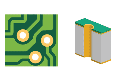
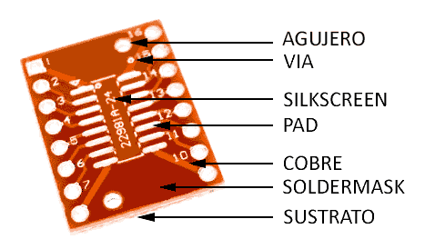
 What remains to be seen is how the conductor layers communicate vertically, and this is where vias come into play. A Via is a vertical hole, usually small in size, which has copper on its inside and connects the top layer with an inner layer.
Vias should not be confused with the holes in some pads for placing PTH components. Typically, vias have a very small size.
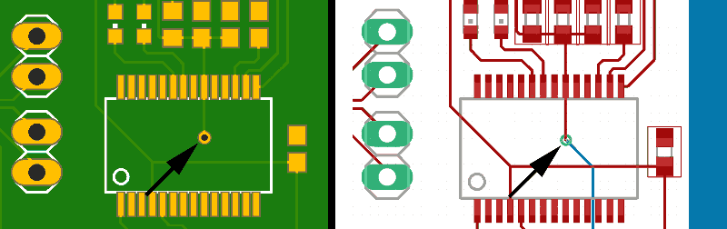
Together, horizontal traces and vertical vias configure the electrical circuits. Therefore, both are equally important in our PCBs.
In fact, we already said in the previous post that, due to mathematics and topology, it can be demonstrated that a single-layer board cannot implement any type of circuit.
If we have a trace crossing, it’s possible we have a geometric arrangement that doesn’t allow us to make all the connections on a single plane.
However, if we have two layers, things change. If we encounter another trace or a crossing, we can place a via, go to the other side of the PCB, and continue our trace there.
On the other hand, we already said that in this series of posts we would focus especially on two-layer PCBs, mainly because they are the ones we can acquire at a low cost.
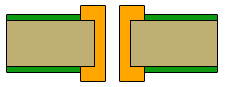
However, we cannot fail to mention that, in the case of PCBs with more layers, there are also vias that connect the inner layers. These are classified into:
- Through, start and end on an outer layer.
- Blind, start on an outer layer and end on an inner layer.
- Buried, start and end on an inner layer.
As we have seen, vias are an essential element that we will inevitably use in our boards. However, generally a good PCB design should minimize the number of vias used.
A good arrangement of components, intelligent and thoughtful trace routing, contributes to eliminating the need to cross from one layer to another.
In fact, it is common that, after finishing designing a part of the PCB, we spend some time thinking if we can find a way to change the routing to reduce the need to go from side to side.
That’s all for this post dedicated to our friends the Vias of a PCB; to understanding their construction and necessity in our designs.
And now that we have seen the most important parts of a PCB, and so we can finally stop being afraid of them, in the next post we will briefly see how a PCB is manufactured. See you soon!
